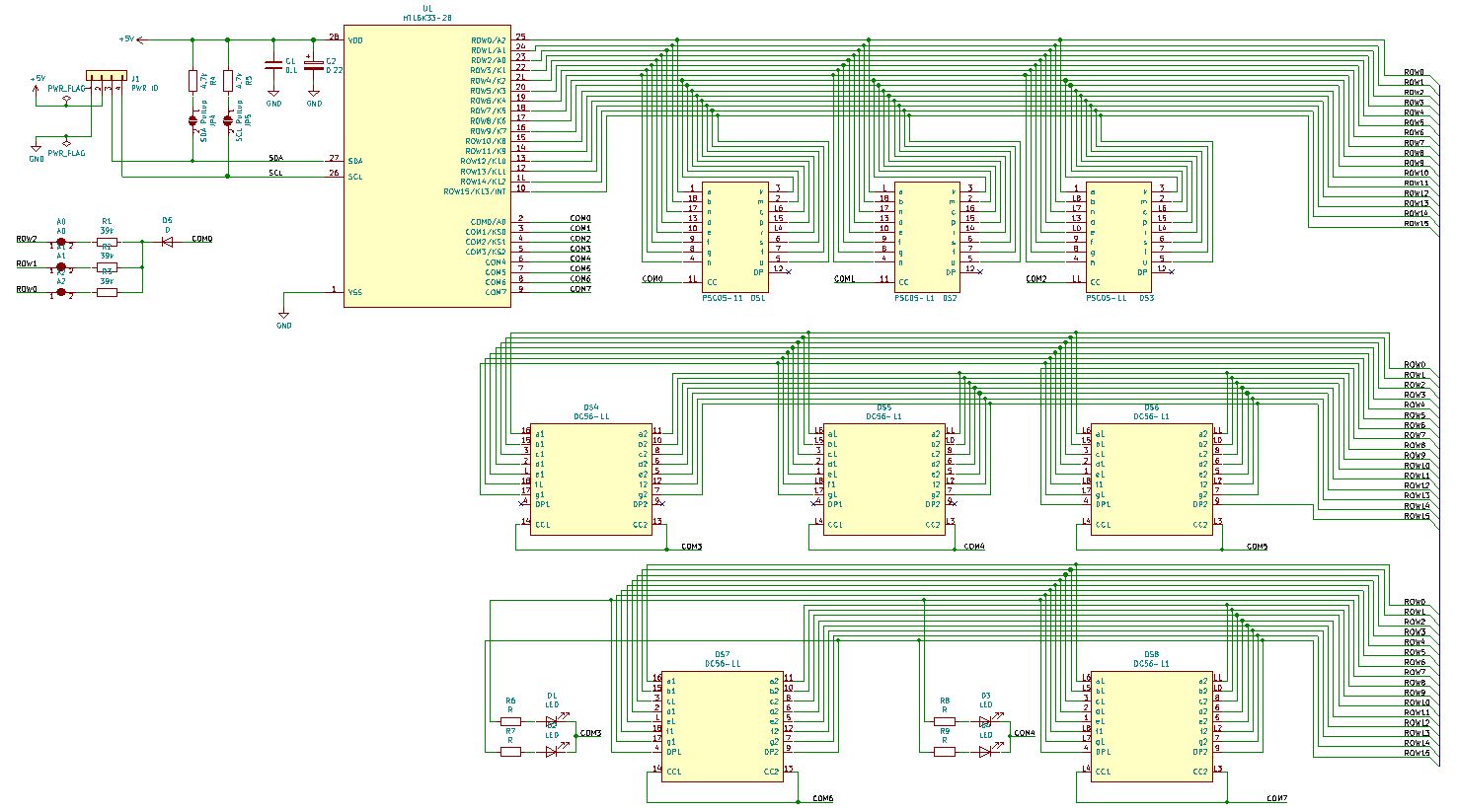
The Display Board Schematic
While it’s possible to make a PCB in KiCad without a schematic, having the schematic will insure that all traces are connected correctly. KiCad shows how everything should be connected in the board layout and makes sure no connections are missed as well as making sure no design rules are violated. The resulting schematic is almost identical to the Parts Not Included schematic, there are not many other ways to do it although ordering of the rows and columns could be optimized for easier PCB layout, they don’t need to be in a specific order.
The HT16K33 has 16 rows and 8 columns. For each column, 16 LED anodes are connected to the rows and their cathodes are connected to one column. Each column is enabled in sequence while while rows needed to select the desired LEDs for the current column are enabled.
Which rows are enabled are determined by pairs of bytes in memory locations of the HT16K33. A bit set to 1 will cause the corresponding LED to light. Displaying letters or numbers will be simple mater of writing bit patterns to the memory corresponding to the LED segments to light.
With the alphanumeric displays, 1 column selects the display and the 16 rows drive the 16 segments. For the numeric displays, 1 column selects two 7 segment displays, the first 8 rows control the first display, and the second 8 rows control the second display. Since only 7 bits are needed per digit, extra row/bit per digit is available. This extra row/bit is used for the colons, AM/PM indicators, the rest are connected to the decimal points, which aren’t currently used.
The Display PCBs
Due to the complexity of the wiring involved, the need for a two sided board and number of holes, this board will need to be professionally manufactured. I’ve made many single sided boards by hand, this will be my first time having one made.
KiCad was used to lay out the the boards. Footprints were made for the Kingbright LED displays using measurements from the datasheets. The dimensions were again used to precisely position the displays on the board. These dimensions and LED positions dictated the size of the boards. The board needs to be as small as possible, but provide enough space for mounting holes and connectors.
This is also my first time using KiCad for anything serious. I’ve only used it for one other small home made board previously. It’s difficult at first, but is not hard to learn and proficient in. There are plenty of tutorials and videos. The DigiKey YouTube series on KiCad covered everything needed to get started laying out the board and the specific details needed to prepare it for manufacture.
This board took over 10 hours to lay out, not an easy first time board. The second board was made by copying this one and changing the alphanumeric footprint for the alternate pin-out of the yellow displays. This took another 3 or so hours.


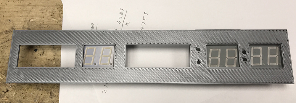
KiCad allows for precise positioning of components on the board. The top layer copper layout was printed on paper to hold up to the 3d printed test print to verify everything was aligned and centered properly. I had some 2 digit LED displays with the same dimensions of the one that would be used, these were used to help confirm alignment. I didn’t have the alphanumeric displays yet and was going only by the datasheet dimensions.
Testing with similar LED displays:
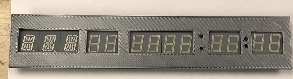
Testing with the real LED displays, everything lines up as it should: