Assembling the Boards and Testing
With the PCBs and LED displays and other parts, I was ready to assemble and test a board. LED displays were initially inserted, but not soldered, to test for positing and fit and were aligned. The result was a perfect fit, careful measuring and double/triple checking paid off.
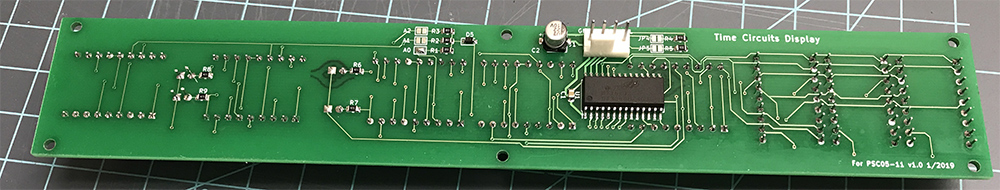
Surface mount components were soldered first using solder paste and hot air rework methods. Next the first alphanumeric LED display was inserted and soldered.
Before the display will do anything, some software needs to be written first to test it. An Arduino Uno was programmed with a test program to initialize the HT16K33 and turn on all of the LEDs. The result… it worked! The rest of the LEDs were installed and tested, everything seemed to work as expected.
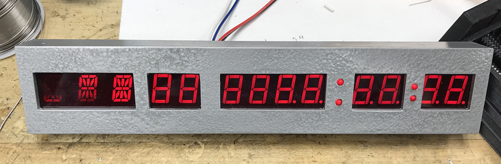
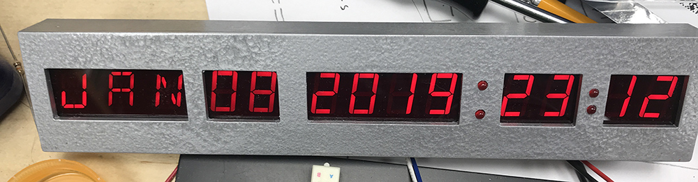
Here’s a photo of the display board in a test print front panel with red transparent acrylic plexiglass filters. Unfortunately I didn’t take a picture of the completed first board out of the enclosure. The first display is lit, but looks dark due to it being multiplexed and the camera’s shutter. I spray painted this 3d part to test the hammered paint, which appears to be used on the real time circuits. This display is built to scale and painted.
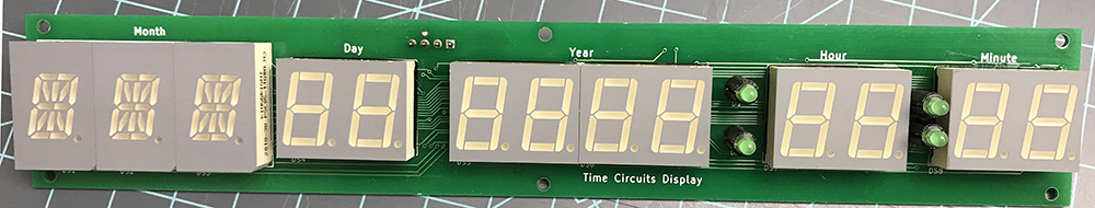
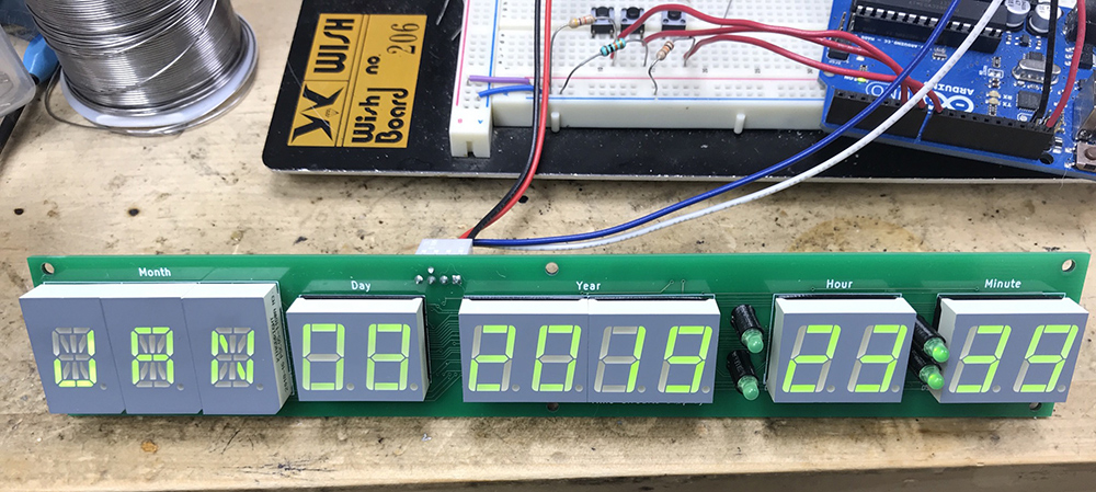
This is not the first board, but one made later showing construction:
At this point I had also had the initial software written to read the time from the RTC and send it to the HT16K33 for display using a “font” created in an array using the datasheets in the schematics.
This is where I discovered a problem with the PCBs. Two segments on the alphanumeric displays seemed switched with each other. Double checking the schematic, board layout and datasheets seemed to indicate everything was connected as it should.
 The problem turned out to be an error in the creation of the footprints for the display. The footprints describe the physical size and holes/pads (and their numbering) for a component. Pins 16 and 17 were swapped. These displays follow the typical counter clockwise pin numbering that most ICs use. I somehow switched 16 and 17 when making the footprint. This resulted in everything appearing to be connected correctly – it was connected as the footprint dictated, which was incorrect. Luckily these two pins are both LED anodes, so only a simple modification to the LED patterns in the software was needed. Additionally these two segments/pins are the same on both pin-out versions, if they weren’t the software would have to correct for this when accessing the yellow display. The footprint has been corrected, but now “purposely” mis-wired in the schematic so it matches the real boards (and any future ones.) There’s no real “right” order for the rows/anodes away.
Here are the display boards displaying time retrieved from the RTC:
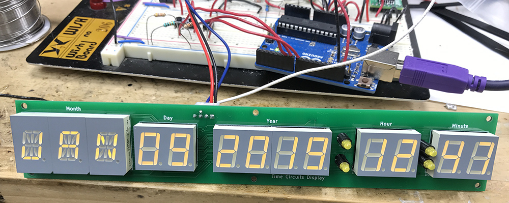
The displays look best in normal indoor lighting, it’s bright in my workshop and they look a bit dim as a result.